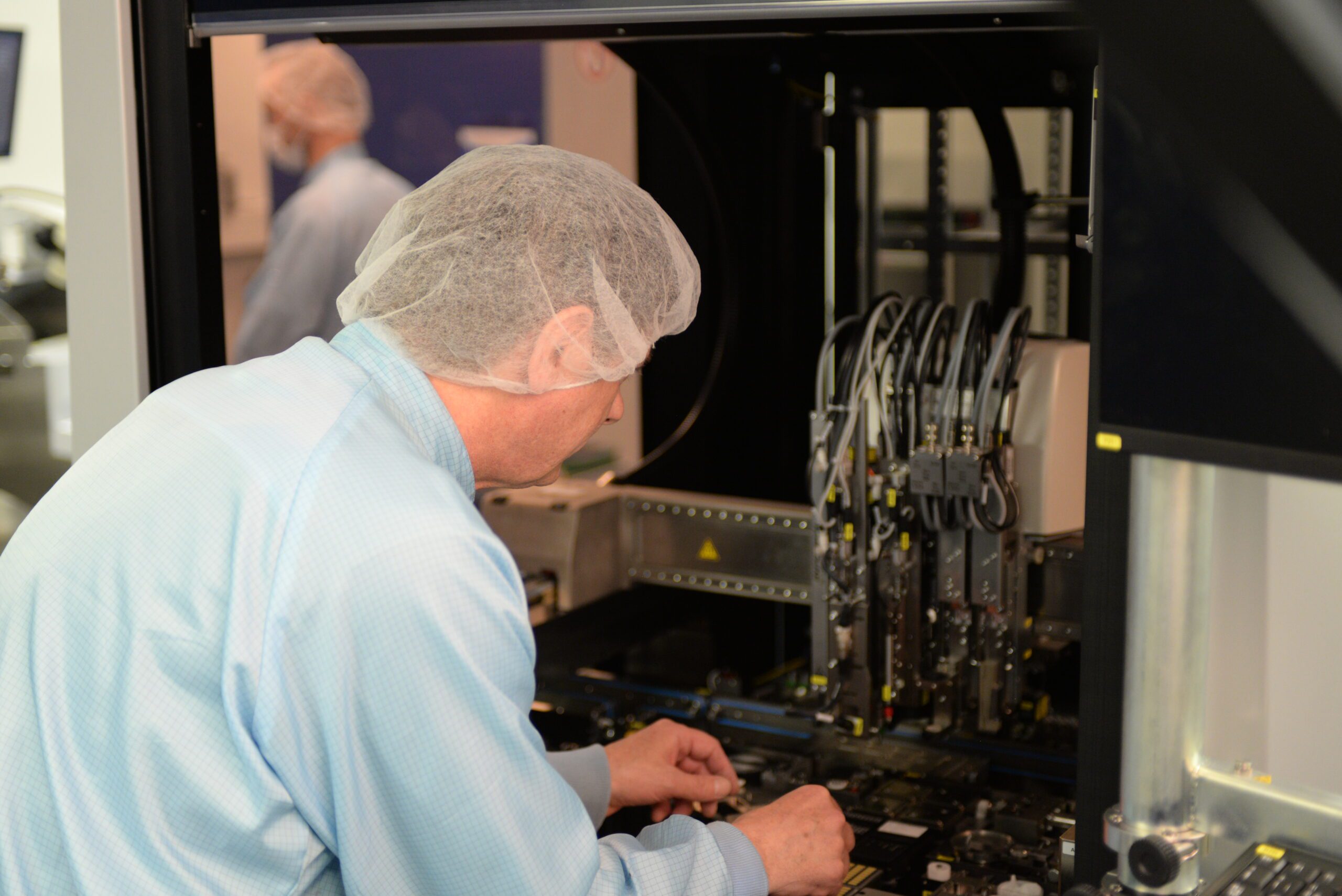
Die bonding
With die or chip bonding it is possible to place components such as integrated circuits, sensors, MEMS and optical sensors on a printed circuit board. During the die bonding, an electrically conductive or insulating adhesive is applied by means of dispensing, jet, stamping or dipping technology before the component is positioned with micrometre precision. During the final step the adhesive is thermally cured, either in an oven, by heat-sealing or under UV light.
Unlike with SMD technology, die bonding allows for the assembly of semiconductors that come directly from a wafer. This significantly reduces the time-to-market phase. This technology is ideal for manufacturing prototypes for pilot runs and for medium-sized production batches. Die bonding is unbeatable when it comes to building multi-chip modules. Die bonding offers a major advantage when working with high-power LED modules as the thermal coupling of the naked LED chips to the substrate is optimal.
Since 2022, Altatec has been the proud owner of a custom-made die bonder that is amongst the most flexible and modern in the world. Alongside the standard functions, it also offers new options that are tailored to our needs.
Technical properties
- Force- or movement-controlled assembly
- Flip chip (180° and 90°)
- Freely programmable dispensing pattern with integrated volume control
- Dispensing methods: Standard and precision time/pressure dispenser, screw dispenser, jet dispenser, stamp and flux dispensers
- Processing of wafers with a diameter of up to 12”, waffle packs, gel packs and SMD reels
- Substrate and bond head heating for the in-situ soldering of BGAs
- Suitable for assembling micromechanical components, such as optical components, reflectors and MEMS
- Integrated UV light source for the in-situ curing of UV adhesives
- Precise height measurement by means of tactile or contactless sensors
Specifications
Applications
- Assembly of chips precise to the micrometre, for prototype manufacturing through to mass production
- Assembly of micromechanical and optical components such as lenses, reflectors, MEMS or optical-electronic systems
- Thermocompression bonding
- Assembly and in-situ UV curing of optical components
- Miniaturised systems, such as stacked chips (chip-on-chip, stacked dies) or multi-chip modules
