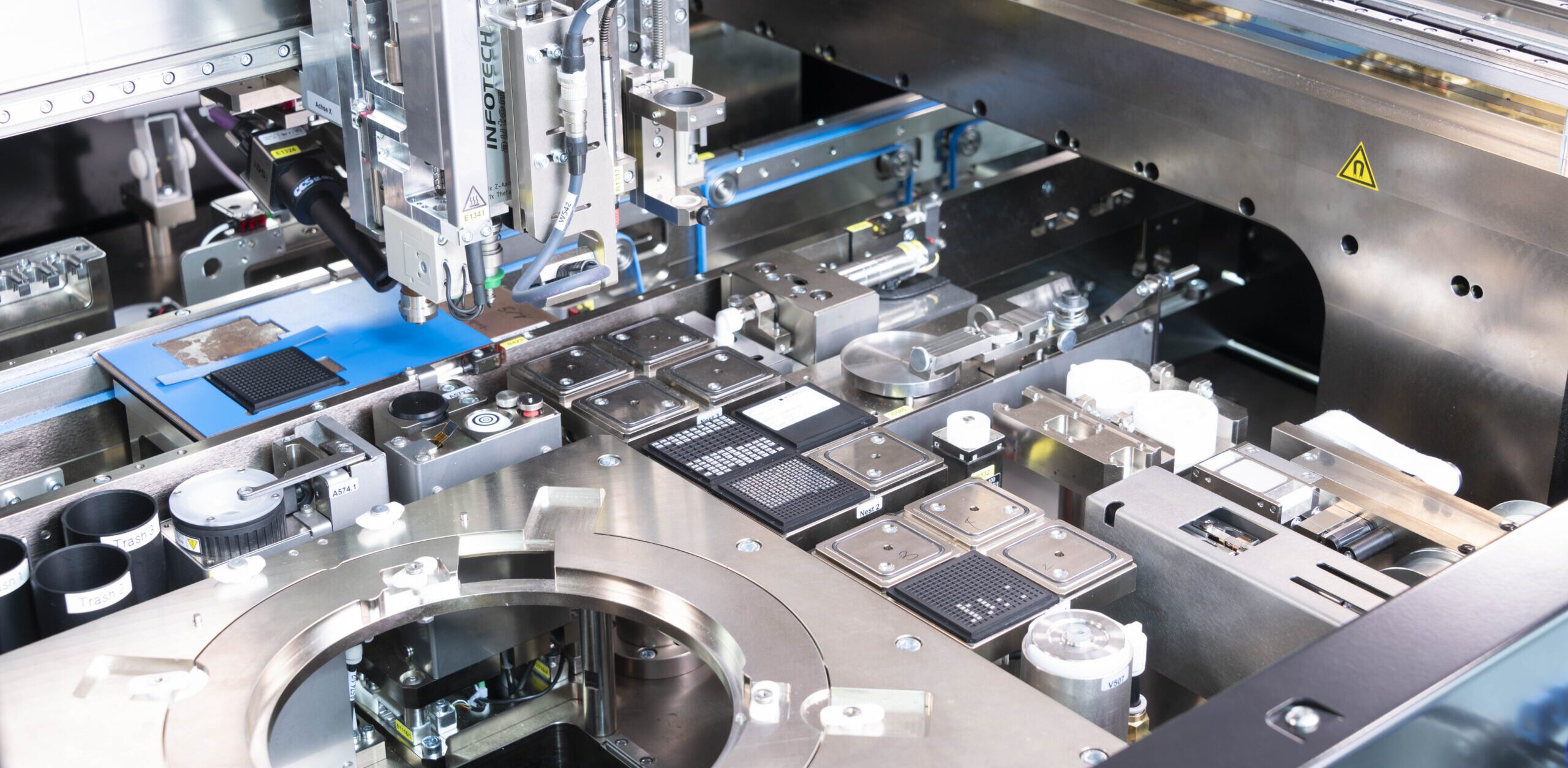
Chip assembly
With Chip On Board assembly, unencapsulated semiconductor components are assembled directly on a substrate to create an electronic assembly. The individual components are then electrically bonded to the substrate or directly to each other by varaity processes. With the chip and wire technique, the chip is first attached to the substrate through die bonding and is then electrically contacted to the substrate through wire bonding. Alternatively, with the flip chip method the chip is electrically bonded to the substrate either via contact surfaces with anisotropic adhesive (ACA bonding) or directly through soldering.
The advantages of chip technology include the high integration density and the flexible design of assemblies. For example, this technology can be used to build very compact, high-power LED modules, which is not possible with pre-encapsulated LED modules. By combining different chips with a range of different functions into a single system, a so-called system in package or SiP, complex circuits can be built in a very small amount of space. By stacking chips on top of each other (stacked dice packaging), a high integration density is also achieved in the third dimension.
Another advantage concerns the clock rates with high frequency applications, such as with RFID systems. In comparison to classic SMD assemblies, chip bonding technology allows shorter electrical connections between chip and substrate. COB technology-based circuits can therefore operate at higher clock rates than SMD technology-based circuits.
This type of chip technology proved to be ideal during the development phase of semiconductor chips. Newly developed chips are often not available in encapsulated form straight away or are only available as bare die due to the low production quantities.
Applications
- High-power LED modules with a mixed assembly consisting of LED chips and/or other components, such as protection diodes and damping components
- Sensor and actuator systems with analogue, logic and power components
- MEMS
- CMOS camera modules
Typical chip assembly process
-
Die bonding
With die or chip bonding it is possible to place components such as integrated circuits, sensors, MEMS and optical sensors on a printed circuit board. In die bonding, an electrically conductive or insulating adhesive is applied by means of dispensing, jet, stamping or dipping technology before the component is positioned with micrometre precision. Depending on the adhesive, the final step is curring thermally in an oven by means of heat-sealing, or under UV light.
-
Wire bonding
Wire bonding refers to a bonding technique used in Chip On Board technology whereby a thin wire is used to bond the connections (pads) of an integrated circuit (IC) with the substrate. There is a range of different wire bonding methods, some of which use ultrasonic and some of which do not.
-
Adhesive bonding
The adhesive bonding of components has become more important in recent years and presents various advantages and challenges when it comes to semiconductor assembly. Almost all materials can be bonded either to the same material or to other materials. By choosing the right adhesive, curing temperature and time, you can achieve very gentle, electrically or thermally conductive and insulating adhesive bonds.
